

Low-Voltage Electroadhesion: How Nanoscale Gaps Become Measurable Forces
Why the smallest gaps can control electrical attraction
Applying a voltage between two surfaces can make them attract each other. This electroadhesion is useful in handling, positioning and gripping, but it can also create unwanted friction. The strength of the attraction depends not only on voltage: it depends critically on the distance across which that voltage drops.
Real engineering surfaces are rough. Even when they appear to touch, small contact patches are surrounded by gaps of different heights. Replacing that geometry with a single large separation can miss the regions where the electric field is strongest. Conversely, assuming that an entire device has a uniformly tiny gap can greatly exaggerate its force.
Peng and colleagues studied this problem at oxidized silicon interfaces. Their final 2026 paper connects a rough-contact calculation to an electrical model and friction measurements. It provides a useful example of how a mechanical gap field can support another physical calculation, while also revealing behaviour that the simple electrical model does not explain.
The investigated silicon contact
The principal experiment used a 3 mm diameter polysilicon ball against a monocrystalline silicon wafer. Both surfaces carried native oxide layers. The external normal load was 40 mN, sliding speed was 0.1 µm/s, and the dry chamber had approximately 0.8% relative humidity.
The wafer bias was varied between −30 and +30 V relative to the grounded ball. Friction increased under positive bias but remained close to its zero-bias value under negative bias. Additional experiments changed wafer doping, replaced the ball material and examined wafer-on-wafer contact. Those controls helped distinguish geometry from electrical transport effects.
The force measured during sliding was friction, not a direct pull-off measurement of the complete ball–wafer interface. The authors inferred an electroadhesive contribution using a stated relationship between friction and repulsive normal loading. That distinction matters when interpreting the later model comparison.
Why a rough-contact calculation was needed
The ball diameter and external load describe the overall contact, but do not specify the nanoscale separations around individual asperities. Those separations determine the local electric field. A spatial mechanical calculation was therefore needed before calculating attraction across the noncontact regions.
The source cites the TriboSolver download page in reference 32 and describes elastic boundary-element contact calculations. The calculation resolved the deformed interface rather than replacing its gap distribution with one average value. This article describes that published workflow, not a new reproduction using the current release.
Inputs, outputs and the loading convention
| Model element | Information used in the study |
|---|---|
| Contact bodies | Oxidized polysilicon ball and monocrystalline silicon wafer. |
| Geometry | 3 mm diameter ball; spatially resolved rough-interface geometry. |
| External normal load | 40 mN in the main friction experiment. |
| Mechanical calculation load | Repulsive load inferred from biased friction and the zero-bias friction proportionality; not simply 40 mN at every voltage. |
| Surface input and resolution | Measured contact geometry; exact topography processing and grid require the supplementary numerical methods. |
| Elastic properties | Not specified in the main-text method; supplementary values have not been verified for this draft. |
| Contact model | Elastic boundary-element model resolving the full spatial gap distribution. |
| Main mechanical outputs | Deformed interface geometry, contact mask and noncontact gaps. |
| Electrical calculation | Local field and Maxwell attraction integrated over noncontact pixels; oxide thickness 2.2 nm, dielectric constant 3.9. |
Electroadhesion adds to the externally applied load. Mechanical equilibrium requires the repulsive contact force to balance both. The authors estimated that repulsive force as the measured friction force divided by the zero-bias proportionality. Using only the externally imposed 40 mN would therefore represent a different calculation at biased conditions.
This also means the published comparison is partly informed by the friction experiment. It is not a completely independent, voltage-only prediction of both force and friction. Reproduction requires the actual surface data and the same loading convention, as well as the electrical inputs.
From local gap to electroadhesive force
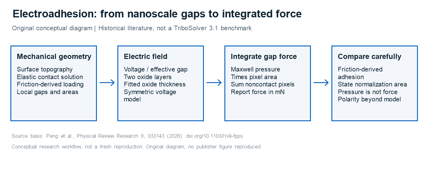
The authors treated each noncontact region as a local capacitor. The electric field was calculated from the applied voltage divided by the sum of the air gap and an effective dielectric thickness. For two oxide layers, that effective thickness is 2d/κ, where d is oxide thickness and κ its dielectric constant.
The local attractive pressure was then calculated as one-half of the vacuum permittivity multiplied by the square of the field. Multiplying this pressure by each pixel’s physical area and summing over the noncontact mask produced the total electroadhesive force. The pixel area and the contact mask are therefore essential parts of the calculation.
The oxide thickness of 2.2 nm was fitted; it was not presented as an independently measured input for every test. The authors neglected capillary adhesion under the dry conditions and estimated van der Waals attraction to be too small to dominate this comparison. These are study-specific modelling decisions, not a statement that other adhesion mechanisms never matter.
What the comparison shows—and which units it uses
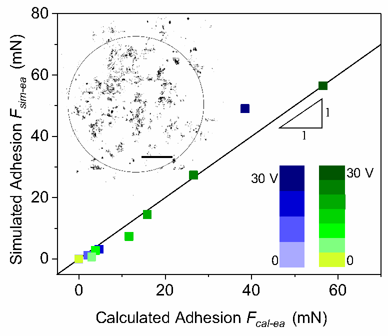
Figure 2 compares the modelled force with adhesion inferred from the friction measurements. Both axes are in millinewtons (mN). The positive-bias comparison supports the combined mechanical and electrical interpretation under the paper’s assumptions.
The separately discussed pressure approaching 100 MPa is normalized over a microscopic contact footprint. It is not a force and is not a pressure delivered uniformly across a macroscopic device. As a unit illustration only, 10 mN divided by 100 µm² equals 100 MPa. This arithmetic is not a new simulation or an exact reconstruction of a plotted point.
Consequently, a few millinewtons in another calculation cannot be judged too small merely by comparing it with a pressure headline. First match the voltage, measured surface, gap processing, oxide convention, repulsive loading, mask and physical area. A different roughness map can change the distribution of the smallest gaps substantially.
The unresolved polarity effect
The simple field-pressure expression depends on voltage squared. By itself it predicts the same attraction for equal positive and negative voltages. The ball–wafer experiment did not behave that way. The authors therefore investigated charge transport and trapping in polysilicon as an additional explanation.
Capacitance measurements and material controls supported that interpretation, but the paper states that the macroscopic experiments did not resolve the microscopic origin of trapping. It would be incorrect to advertise polarity-dependent charge trapping as something demonstrated by the symmetric gap-based model.
Practical meaning and conclusion
The workflow could help assess where surface finish, dielectric layers and loading make electroadhesion important in positioning or handling contacts. Its central lesson is to preserve the spatial gap distribution and clearly record the electrical assumptions. Scaling to a larger interface requires a justified surface representation rather than multiplication of a pressure headline by device area.
For the studied silicon contact, the combined model connected nanoscale gaps with positive-bias adhesion and friction. The polarity discrepancy was equally informative: it showed where contact geometry alone was insufficient and where additional material physics was needed.
Reference and further exploration
Liang Peng, Stefan Kooij, H. Tunç Çiftçi, Daniel Bonn and Bart Weber. “Strong electroadhesion at low voltage enabled by nanoscale roughness.” Physical Review Research 8, 033143 (2026). Final publication · Open-access paper. The earlier preprint is not counted as a separate application.
Explore TriboSolver or discuss your electroadhesion application. Any claim of reproducing this paper with a released version must refer separately to the approved numerical verification and exact case configuration.